FPGAs : Working with DPU Part 1
The initial work needed was to create a Xilinx Support Archive that I could use with either the PetaLinux flow or the Vitis flow, allowing me to run localised AI models on the Ultra96-V2.
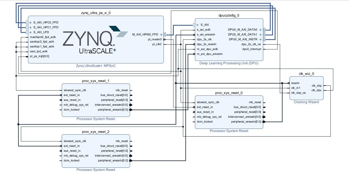
Step 1: Creating the block design
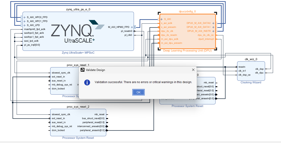
You can see from the image below that I have created a basic block design for the DPU. In the future I need to add MIPI support and DisplayPort output, but for the initial testing of the Vitis AI libraries I felt it was probably best to start off simple.
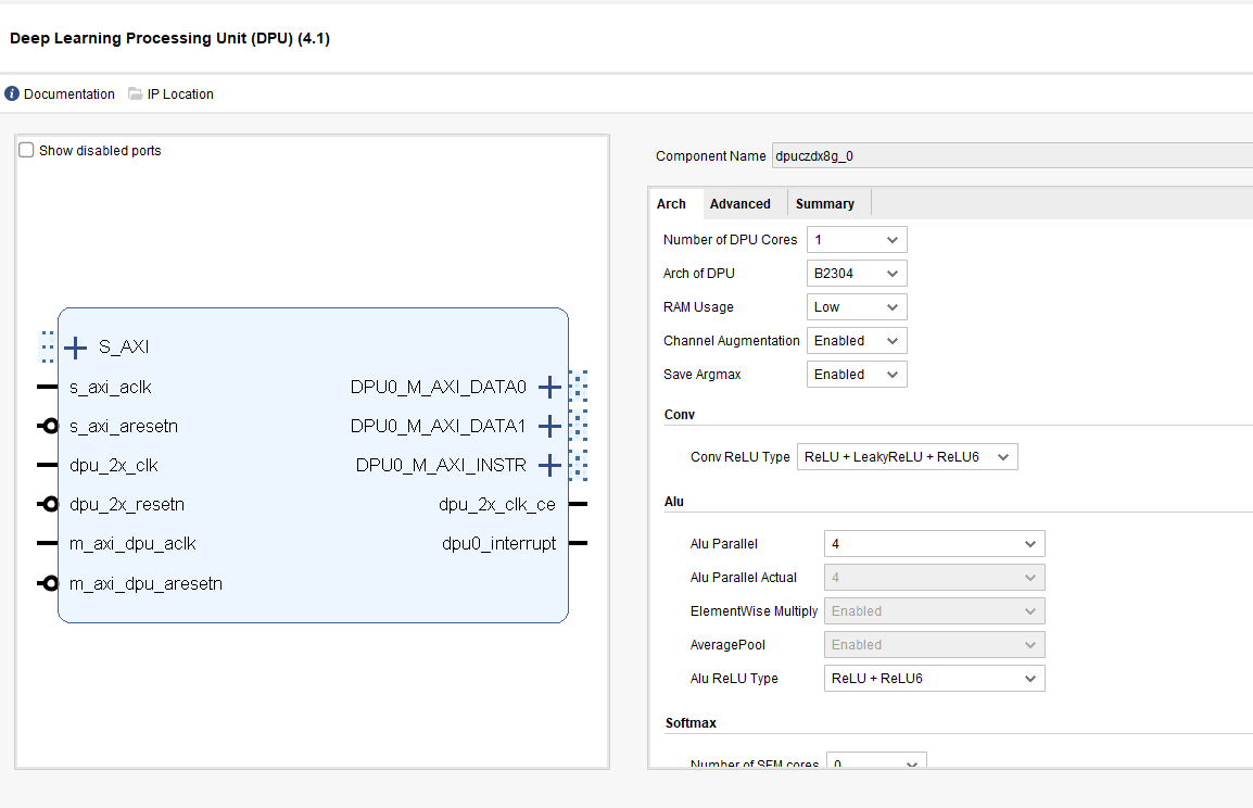
Step 2: Configuring the block design
For the architecture I wanted to make sure I was not using too much of the resources available on the Ultra96-V2, so I set the number of DPU cores to 1 and set the architecture of the DPU to B2304. I also made sure to keep the RAM usage low.
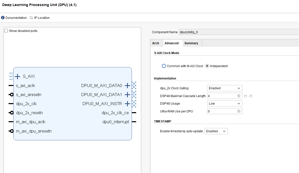
In the advanced settings I enabled clock gating, which allowed the clock for the DSP to be set to “Buffer with CE”. This is the clock that runs the DPU core. I also made sure to keep the DSP48 usage low.
Step 3: Validate Design
There were a few issues with data widths because the slave AXI on the DPU has a width of 32 bits but the master AXI on the MPSoC block was set to 128. Once these were changed it passed the validation, which then meant I could run synthesis and implementation to generate the bitstream.
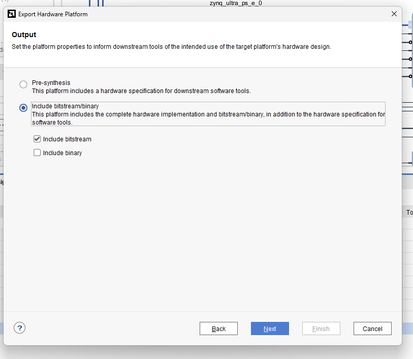
Step 4: Exporting the Hardware Design
The last step of part 1 was to export the hardware platform, making sure to include the bitstream. This will create the Xilinx Support Archive needed by either Vitis or PetaLinux to create the platforms for the Ultra96-V2.